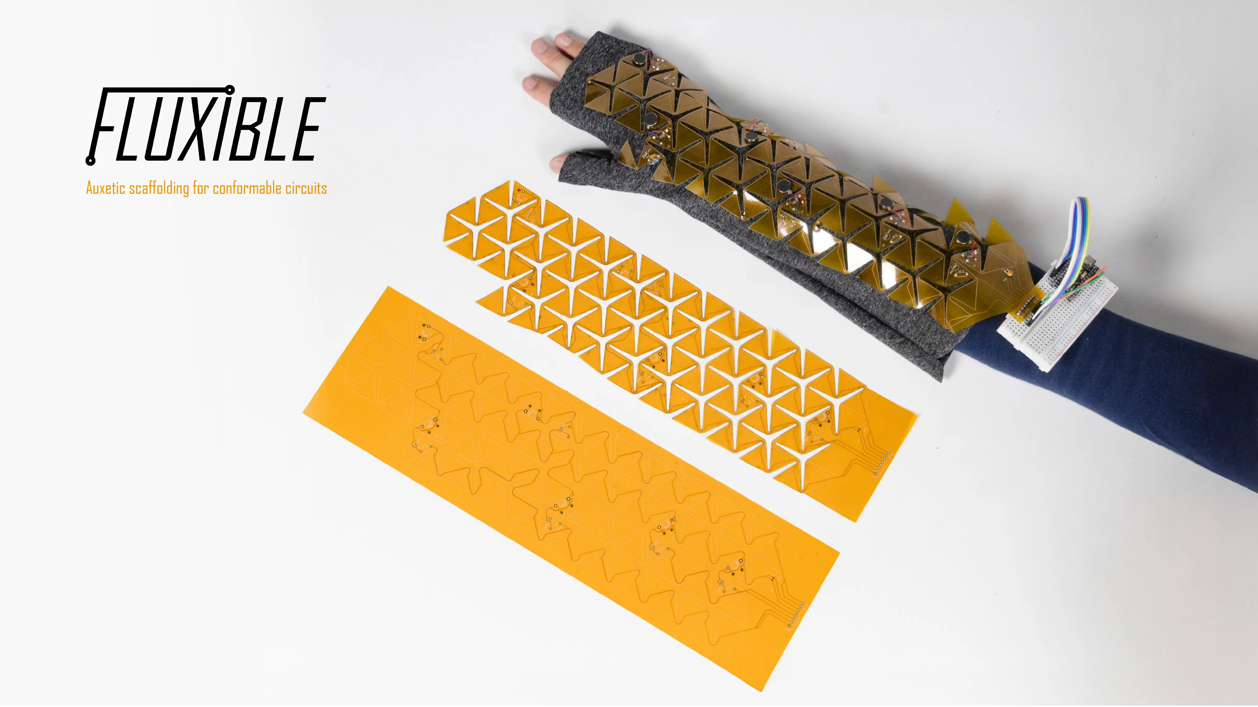
Fluxible
Fluxible is a fabrication method for creating body-conforming circuit boards using auxetic geometry integrated into standard flex PCB manufacturing.
context
design and making ii
team
demi hu xiaoxi xu gloria zhu
timeline
spring 2026 15 weeks
tools
grasshopper kicad arduino
// background
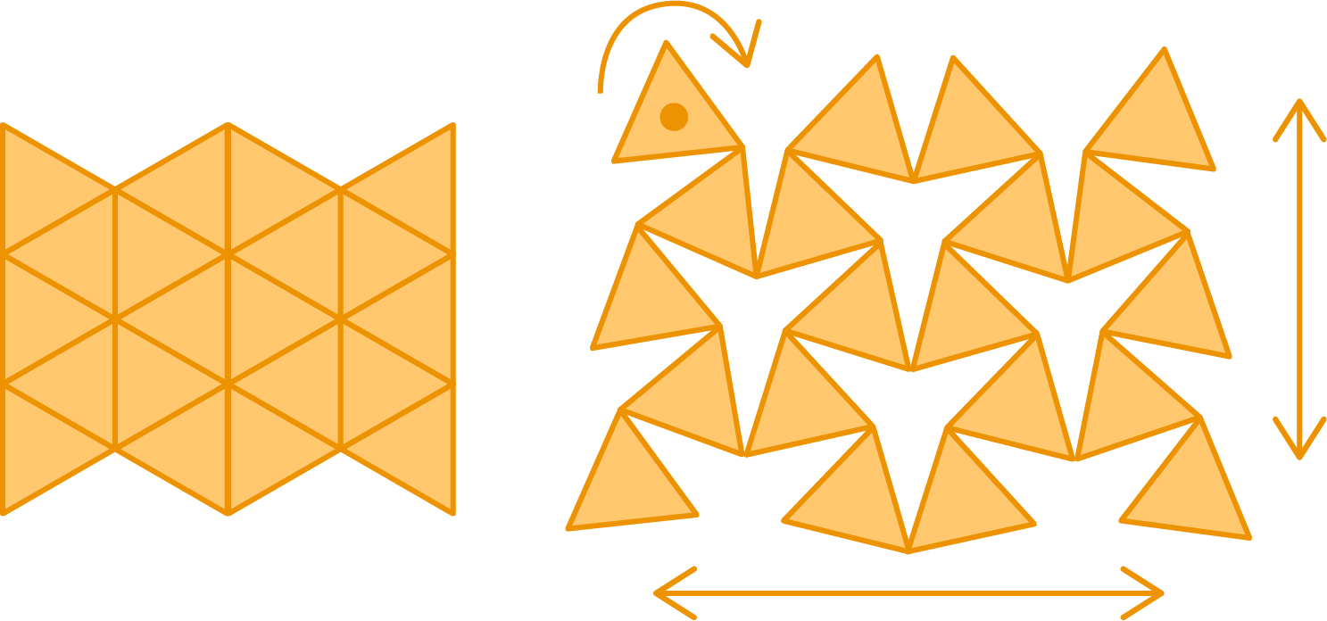
Auxetics: inducing elasticity through geometric structure, not material composition.
Auxetic materials are structures with a negative Poisson’s ratio, so that expansion in the axial direction also causes expansion in the transverse direction. The geometric structures that make a material auxetic are composed of units that rotate locally through the deformation of their hinges, resulting in stretch and conformability over the entire surface.
// problem
There is no unified workflow that combines auxetics + PCB fabrication + wearable electronics.
Wearable electronics are increasingly shifting toward distributed, body-scale sensing surfaces. However, existing approaches struggle to simultaneously achieve mechanical conformability, scalable PCB-compatible manufacturing, and preservation of spatially organized electronic functionality under deformation.
Material-based approaches to flex PCBs, such as using a silicone substrate with liquid metal channels, can be expensive to produce at scale and unsuitable for full-body wearability. Stretch-based deformation also does not handle array-based sensing well. For applications like expandable LED arrays or haptic suits, an auxetic structure can maintain the spatial distribustion of sensors as it expands uniformly.
Cost:
Compatibility with existing PCB manufacturing makes this method fast and affordable for large-scale applications.
Flexibility:
Auxetic patterns can be designed computationally to customize areas of elasticity or component placement as needed.
Array Support:
Uniform expansion maintains the spatial distribution of sensor arrays under deformation and simplifies PCB assembly.
Wearability:
Polyimide is lightweight and auxetic perforations can make it breathable and conform to dynamic, complex 3D forms.
// concept
How might we combine auxetic geometry with conventional circuit printing to create conformable and scalable conductive surfaces?
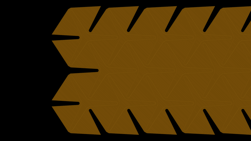
We propose Fluxible, a methodology for designing auxetic perforation patterns to induce customizable elasticity in a standard PCB manufacturing process. Instead of making the conductive material itself stretchable, we use the rotational movement of auxetic unit cells to induce elasticity in a polyimide flexible PCB produced with standard photolithography. We hypothesize that we can design a perforation pattern for flexibility and design circuits to route around these perforations, allowing the material to stretch and conform to complex dynamic forms while only requiring the traces to deform by local bending.
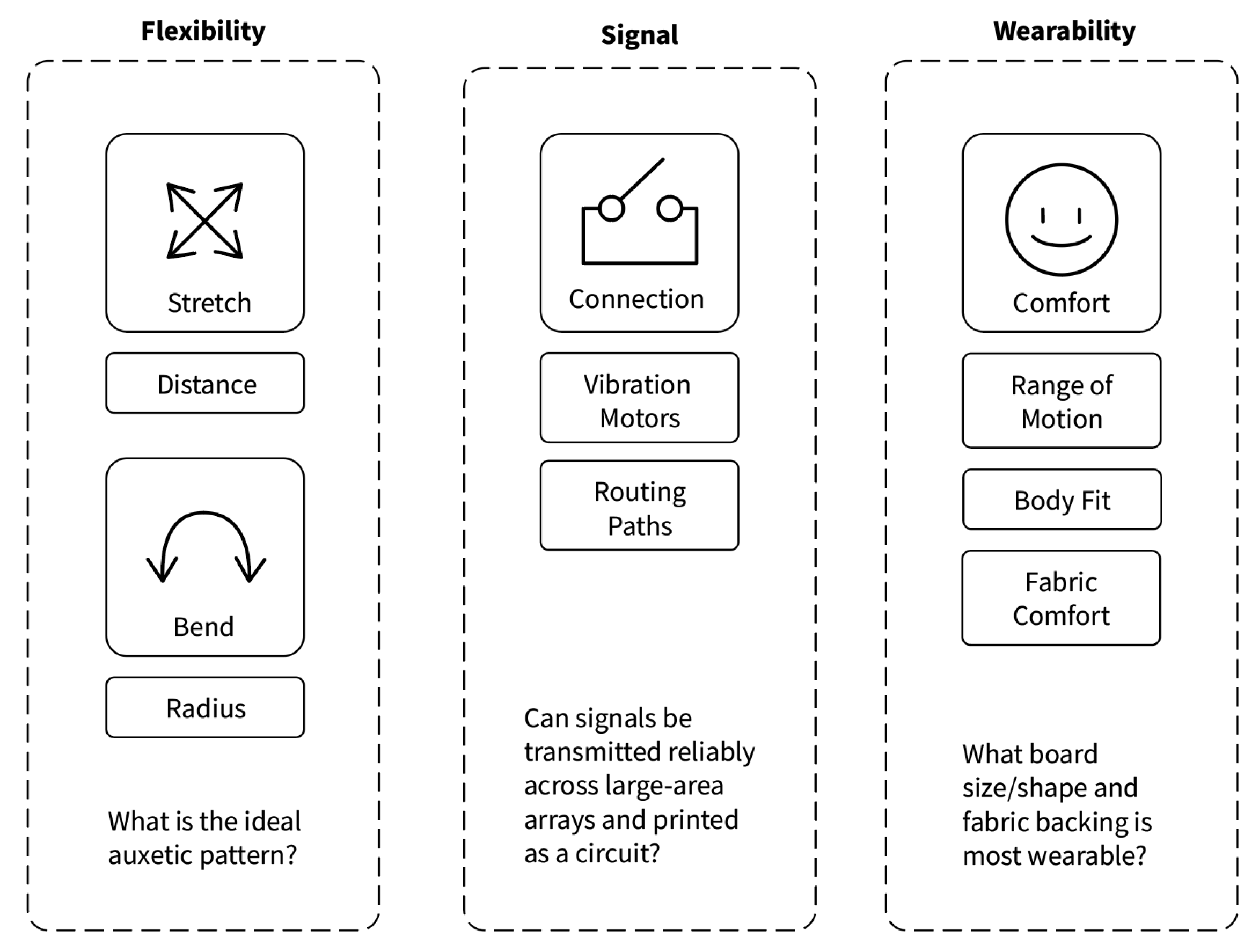
// computational system
Body deformation mapping establishes where and how auxetic perforations are applied.
We perform mesh change analysis in Grasshopper by comparing edge length changes between corresponding mesh vertices on different poses, represented as 3D meshes. The resulting deformation values are mapped onto the body surface to generate a stretch heatmap, which indicates regions that require higher mechanical compliance. This informs our auxetic scaffold parameters and placement within our 2D fabric patterns.
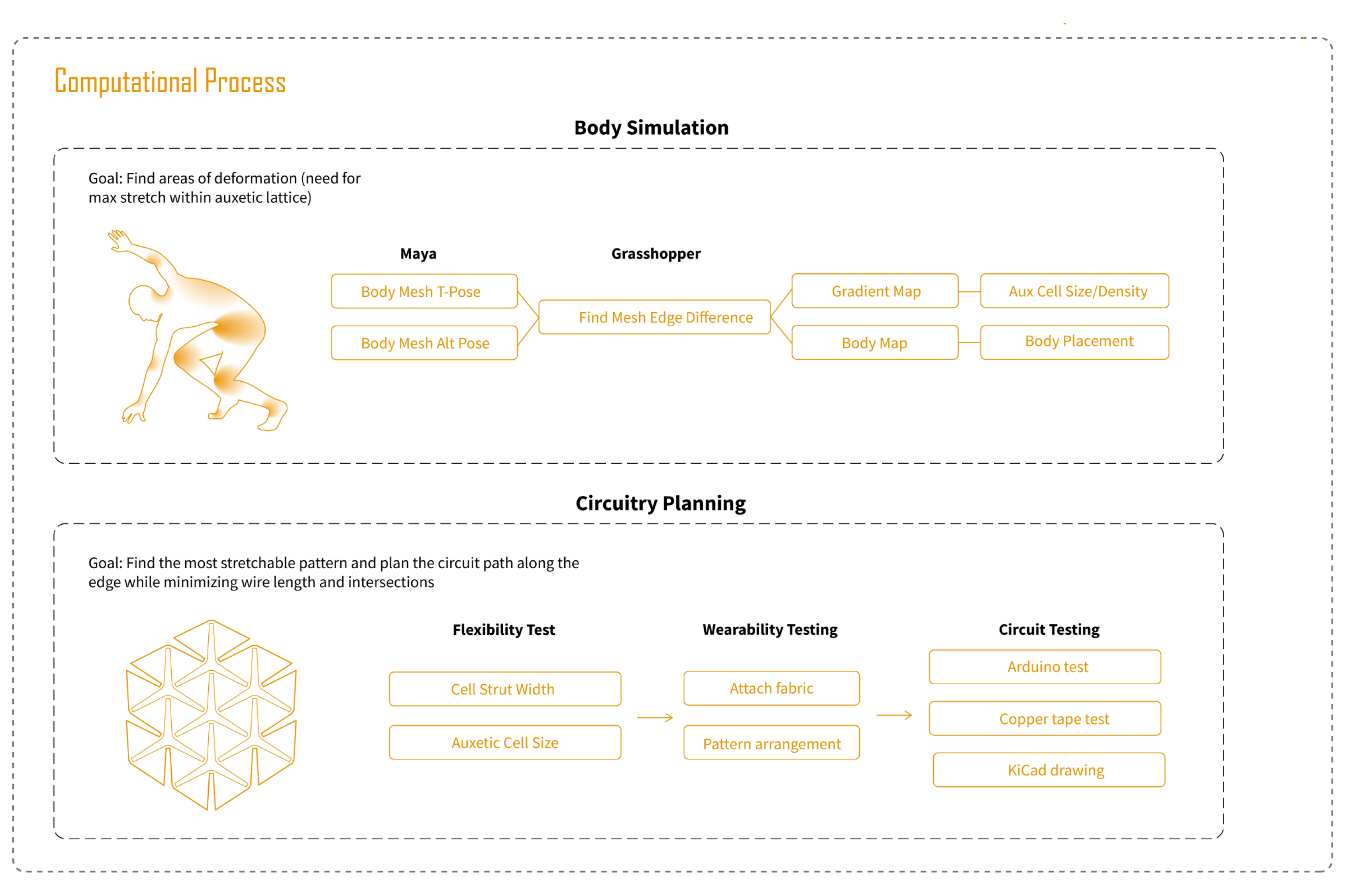
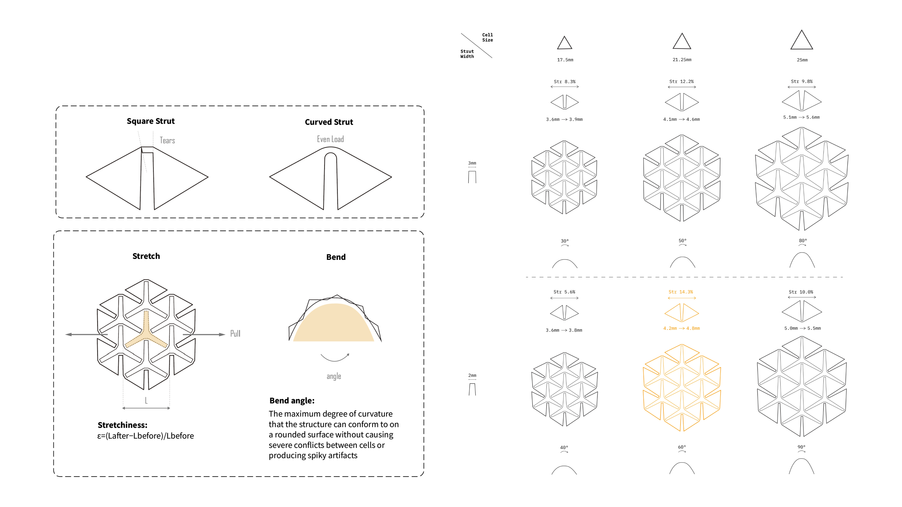
Next, we identified which parameters in the auxetic pattern affected flexibility and strength.
We designed a custom Grasshopper script with independently variable parameters for cell size, strut width, and strut shape. We then produced a series of acrylic swatches to compare how different pattern configurations behaved under manual bending and extension tests. Struts were the hardest to balance: thinner struts allow greater elasticity, but less room to route electric traces.
// methodology
Each stage evaluates flexibility, conductivity, and wearability while keeping compatible with photolithography-based manufacturing.
After identifying the ideal auxetic pattern parameters, we produced sample swatches in various materials and circuit types. We intentionally chose inelastic substrates to better approximate our desired polyimide PCB manufacturing process.
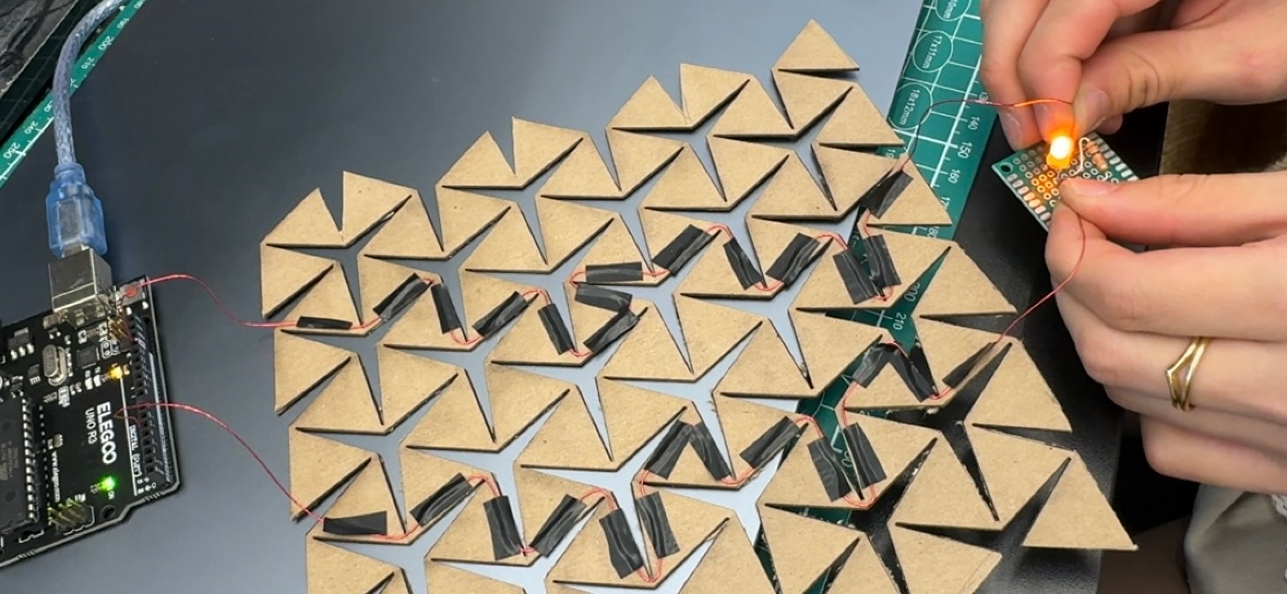
// cardboard + wire
Wire over perforated cardboard confirmed the basic feasibility of routing a conductive path through an auxetic scaffold.
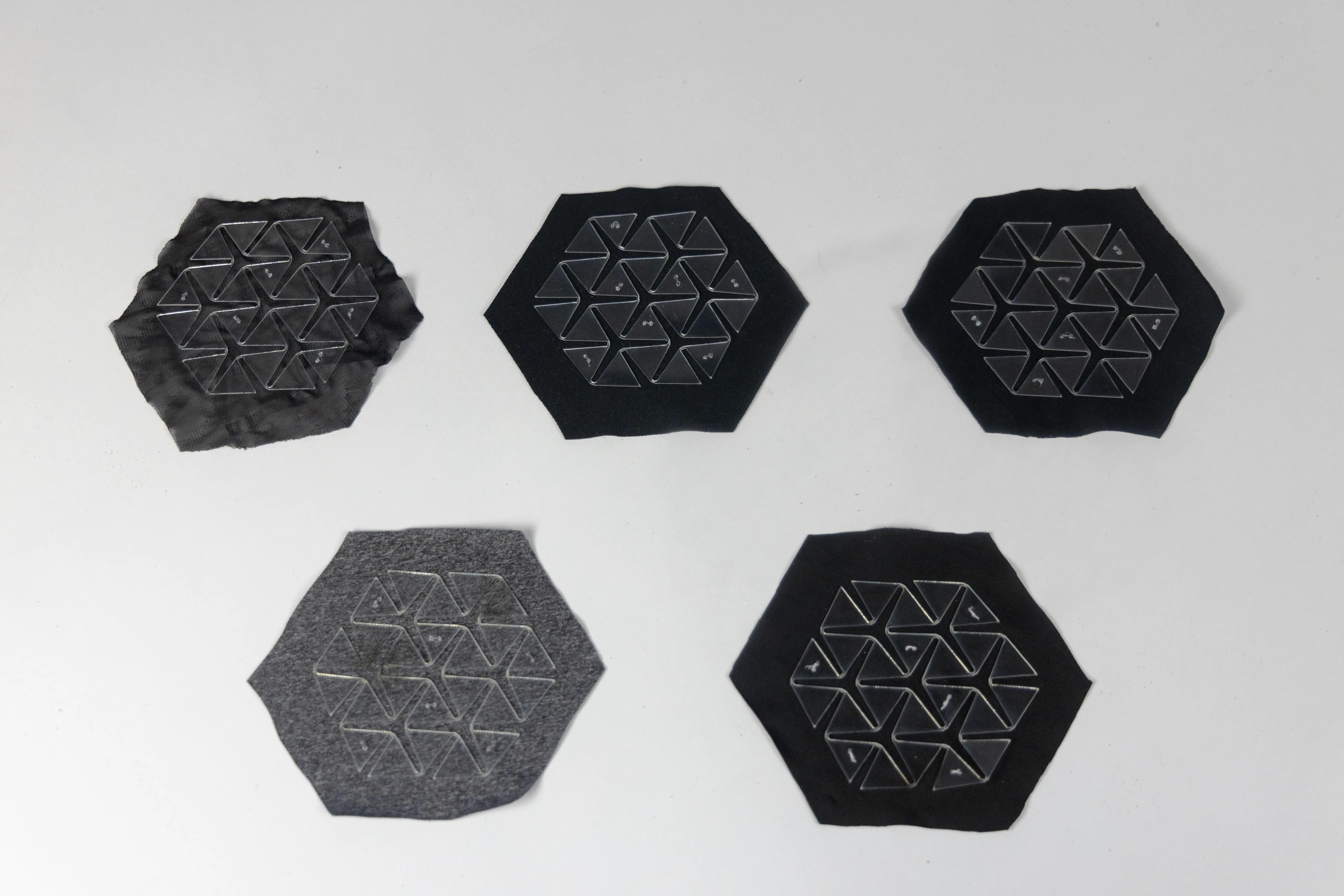
// fabric + acrylic/TPU
Fabric tests revealed that we needed to affix auxetics by the center of each unit to preserve rotation-based expansion.
// acrylic + copper sheets/stencilled conductive paint
Acrylic was our closest approximation to polyimide and helped us test production-ready routing methods.
Rather than manually taping wires to the surface, we were able to digitally design circuit paths along the auxetic perforations and fabricate them with machines. Laser-etching into a mask layer on the acrylic surface created channels we could "screenprint" conductive graphite paint into. Cricut-cutting copper tape into the traces directly was a similar approach.
Neither were quite robust (the paint flaked with deformation, and the tape was extremely fragile to handle), but we were able to create functional auxetic circuit swatches with these methods. Because we used our identified ideal parameters, it also helped us estimate how the strut width would limit the number of traces that could be routed through a single intersection.
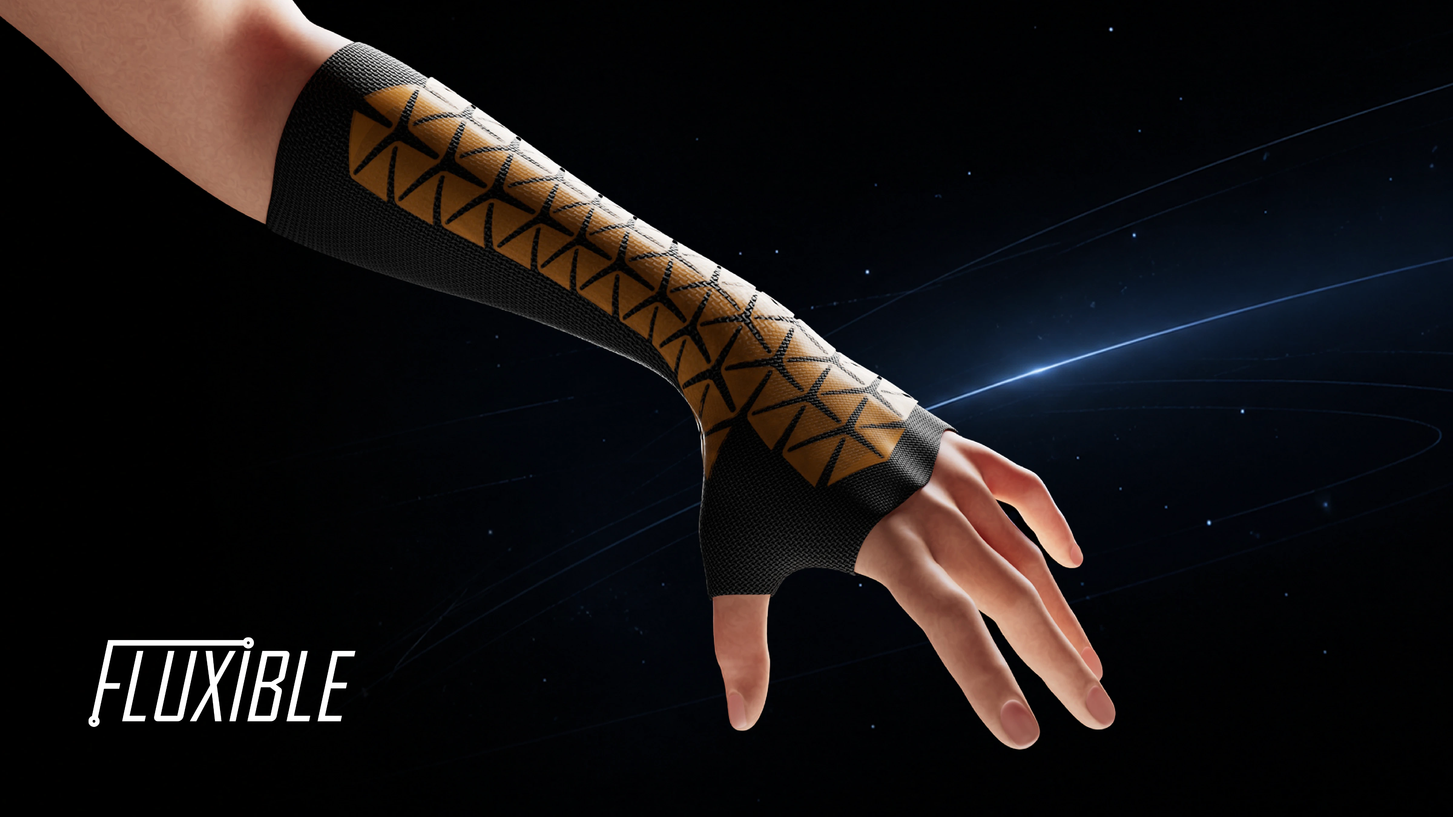
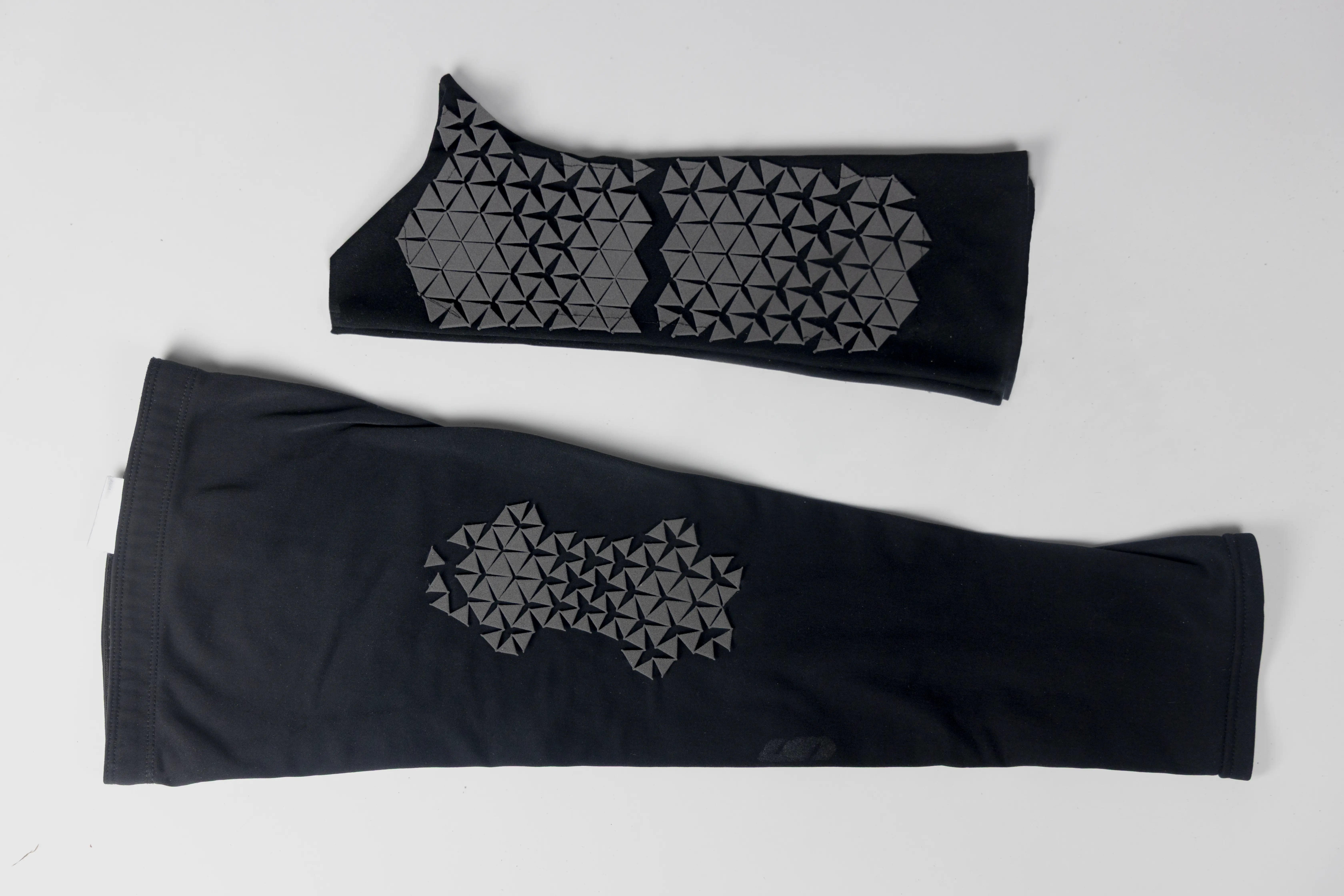
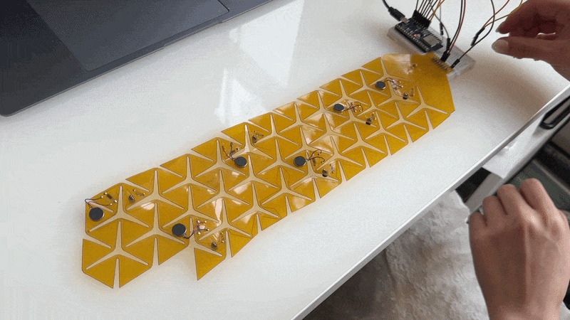
// printed flex PCB + wearable assembly
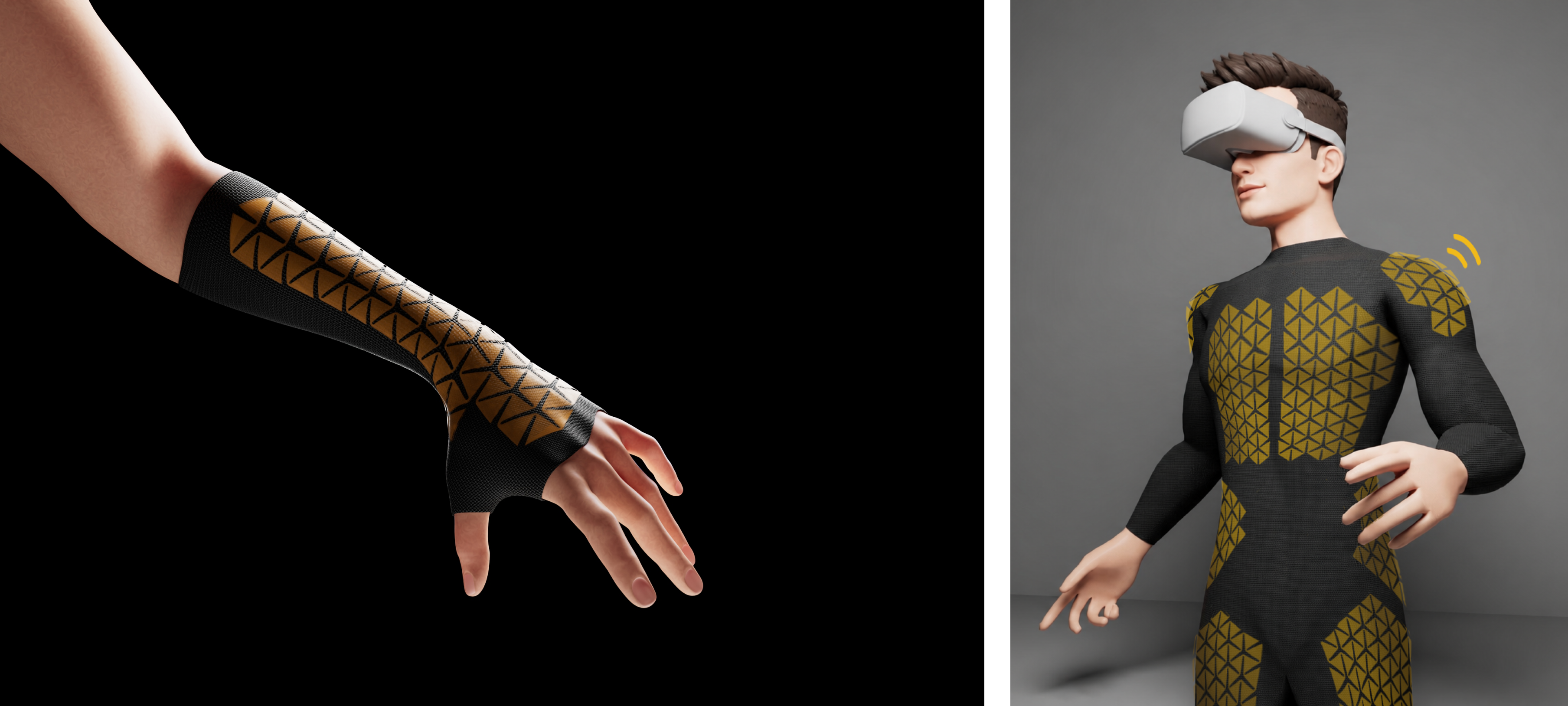
Prototype tests culminated in designing and fabricating a real flex PCB to be used in a haptic glove.
User interviews noted that this methodology would best benefit applications that involve distributed sensing like a haptic suit with an array of vibration motors, rather than isolated electrical islands like a few medical monitoring sensors across a body. There is no reason to maintain a large area of an auxetic conductive surface if it only serves as a "wire" and not an actual circuit board with components.
As a result, we chose a haptic glove as the application context for our final prototype. We developed a glove fabric pattern, then designed the auxetic scaffold to fit fully within a single panel to reduce interference with seams. Six vibration motors were distributed along the length of the glove to create a spatially addressable haptic array. Designing the circuit within the auxetic scaffold introduced unique routing constraints: the perforated pattern divided the PCB into discrete regions suitable for component placement, connected only by narrow struts.
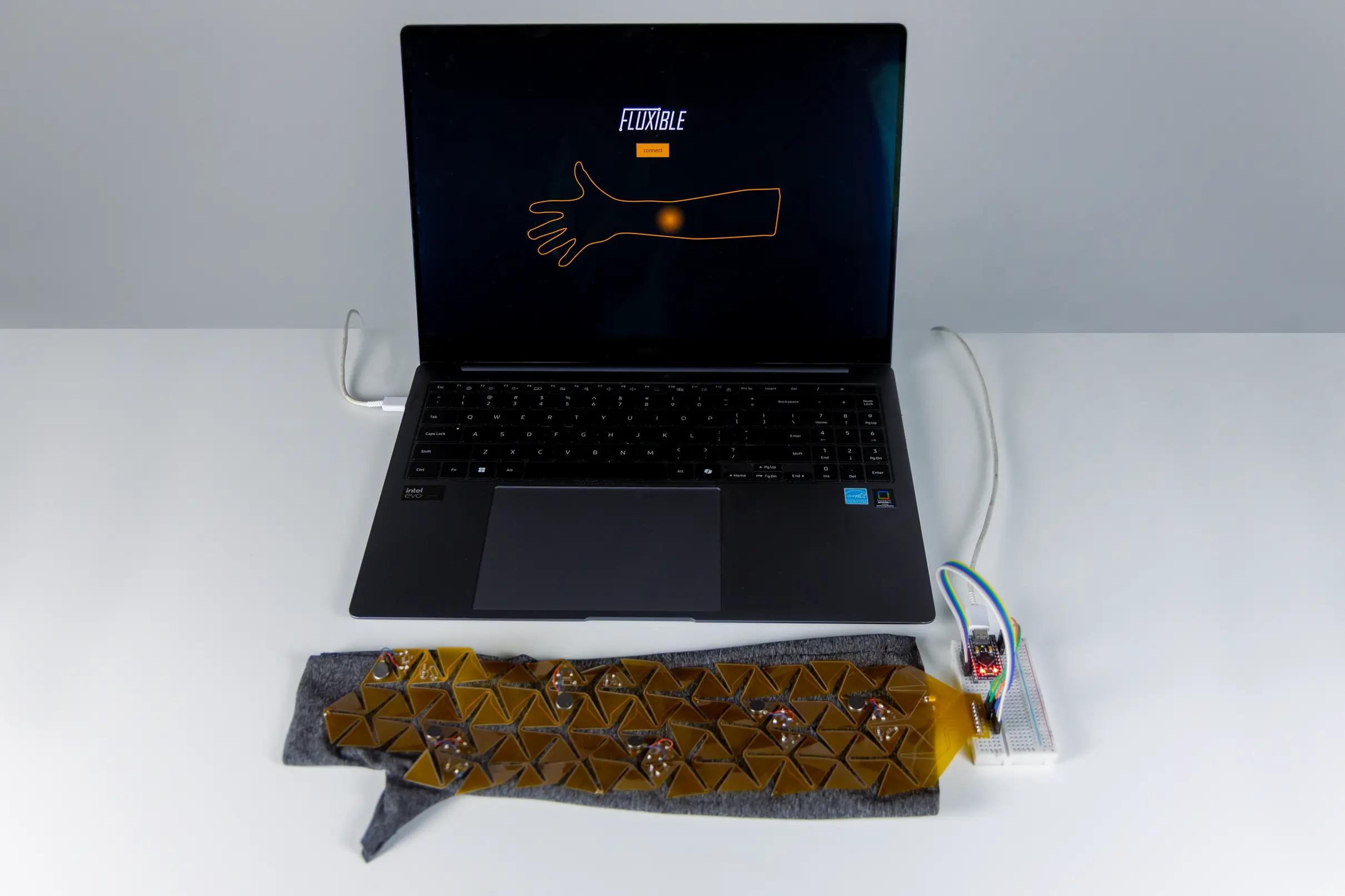
// demo
Connecting an interactive interface mapped digital input to physical output, creating a functional wearable haptic feedback device.
// future work
Combining body deformation analysis, auxetic generation, and circuit routing into a unified computational workflow.
Fluxible establishes the computational foundations for designing conformable circuit boards, but many steps remain manual. Future work would integrate deformation analysis, auxetic scaffold generation, trace routing, and component placement into a single pipeline capable of producing custom wearable electronics for different bodies and applications.
Our final prototype demonstrates the feasibility of integrating auxetic geometry into standard flex PCB manufacturing. While it is comprised of a single wearable module, it sets the stage for future work to investigate interconnected auxetic circuit patches, automated body-specific layouts, and large-area routing strategies, enabling wearable systems that span much larger portions of the body.